| Home | | Products | | Supports | | Shopping Cart | | About us |
 |
|---|
 Member Login
|
|
||||||||||
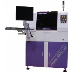
Specification
|
Vision Input Unit
|
|
|
Camera
|
High resolution color 3Mega pixel
|
|
Lighting Source
|
Multi-angle LED dome with PWM brightness control
|
|
Image Resolution
|
15.6μm/pixel
|
|
Frame Extent
|
32mm X 24mm
|
|
Measurement and Diagnoses
|
MultiMetric™ Image analyses method
|
|
Inspectable PCBs
|
|
|
Solder Process
|
Reflow or wave solder
|
|
Size
|
Maximum: 510 x 460 mm
Minimum: 50 x 50 mm
|
|
Thickness
|
0.5 to 2.5 mm
|
|
Clearance
|
Top 24mm Bottom 20mm
|
|
Warp
|
Within 1mm
|
|
Measurement and Inspection
|
|
|
Inspectable Component
|
Chips 0603 and up, LSI 0.3mm pitch and up, through-hole components
|
|
Component Placement
|
Presence/Absence, XYӨ offset, wrong component, Component Orientation, Lifted leads
|
|
Solder
|
Solder bridges, insufficient solder, excess solder, wettability, through hole pins, dropped parts and solder
|
|
Speed
|
About 380ms/frame
|
|
XY Robot
|
|
|
Maximum Speed
|
500 mm/s
|
|
Repeatable Accuracy
|
10 μm
|
|
Conveyor System
|
|
|
Transportation
|
Belt
|
|
PCB Level
|
900(+/-)10mm
|
|
PCB Fixed Method
|
Clamped at rear side
|
|
Direction
|
Right-Left, Left-Right, Right-Right, Left-Left, Bypass
|
|
Rail Width Adjustment
|
By wheel handle
|
|
Interface
|
Support SMEMA 1.2
|
|
Computer Related
|
|
|
P C
|
DOSV PC Windows XP Professional
CPU: Dual core RAM 2GB, HDD 350GB or up
|
|
Language
|
Japanese / English
|
|
Programming
|
|
|
Procedures
|
1. Read the CAD data or Mount data text file to get Part
name, XYӨ, and package, rotation information 2. Using camera auto route tools to set optimal route
3. Verify the coordinate data at the machine
4. Selecting suitable decision limit value.
Training and fine tuning |
|
Library
|
Standard component package library or use package library editor to create customized library
|
|
Others
|
Offline programming supported, multi panels PCB support, top and bottom side inspection at one project file
|
|
Defects Result
|
|
|
Defects Detail Output
|
Contents: Part name, defect location, defect image, etc. Method: Iin file or page print.
|
|
Inspection Result Logging
|
Configurable
|
|
Defect Review
|
Show the full PCB map, defects images and location, etc
|
|
SPC Tools
|
|
|
SPC
|
Statistics of part shift, solder quality value at Cpk, Xbar, and histogram
|
|
Process Warning
|
Warnings : The measurement value is close to the defect level. The measurement value is far away from regular value trend.
|
|
Facilities and Factory Integration
|
|
|
Dimensions
|
W1100 x D1000 x H1600mm |
|
Power Requirement
|
100V single phase 50Hz/60Hz 10A Available for assigning others when PO.
|
|
Air
|
0.4 to 0.6Mpa
|
|
Working Temperature
|
10 - 35℃
|
|
Humidity
|
30 - 80% RH
|
|
Options
|
|
|
OP01 Offline Software
|
For programming, result display at rework station and statistics report confirmation
|
|
OP02 OCR
|
For board and component top characters recognition
|
|
OP03 Barcode Reader
|
Barcode reader for project switching
|
|
OP04 Stamper Mechanics
|
GO/NG stamper
|
| Home | About Us | Contact Us | Terms and Conditions | Copyright @ 2005-2019 Kyoritsu Electric Corp., All rights reserved. |